Advanced semiconductor manufacturing has become an industry defined by heavy capital requirements and high technical complexity. AI GPUs, high performance computing, and data center chips increasingly depend on advanced process and packaging technologies, which is one of the key reasons TSMC has maintained its long term industry leadership.
The TSM business model currently centers on wafer foundry services, advanced processes, CoWoS packaging, customer ecosystems, and AI chip manufacturing. Advanced manufacturing capabilities, stable yield rates, and long term customer collaboration have also gradually become the core of global semiconductor competition.
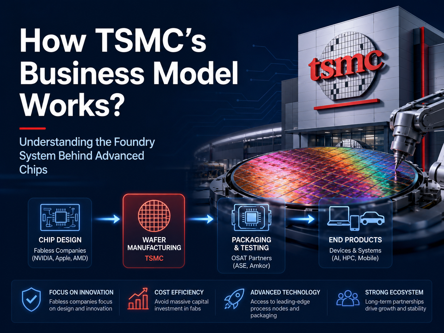
How the TSM Wafer Foundry Model Took Shape
The formation of TSM’s wafer foundry model essentially came from specialization within the semiconductor industry. As the cost of advanced fabs continued to rise, more chip companies began focusing on chip design instead of building their own manufacturing plants.
Fabless companies are mainly responsible for developing GPU, CPU, and SoC architectures. TSMC handles wafer manufacturing, lithography processing, and some advanced packaging processes.
This division of labor means chip companies can concentrate their resources on chip design without taking on fab construction costs that can reach tens of billions of dollars. TSMC, meanwhile, improves advanced process utilization and production efficiency through large scale manufacturing.
Below is the main collaboration structure within the TSM wafer foundry system:
| Segment |
Main Companies |
Core Responsibilities |
| Chip design |
NVIDIA, Apple |
Architecture development |
| Wafer manufacturing |
TSMC |
Chip production |
| Equipment supply |
ASML |
Lithography equipment |
| Packaging and testing |
ASE and other companies |
Chip packaging |
Unlike the traditional IDM model, the wafer foundry system places greater emphasis on industrial collaboration. The development of the AI chip industry has further strengthened the importance of the Fabless and Foundry model.
How Fabless Companies Depend on TSMC to Manufacture Chips
Fabless companies depend on TSMC mainly because of its advanced process technologies and stable mass production capabilities. AI GPUs and high performance chips have extremely high requirements for manufacturing precision and power control.
Companies such as NVIDIA, AMD, and Qualcomm design chip structures based on TSMC’s processes. During the chip design stage, optimization is usually already built around specific process nodes.
In AI GPU manufacturing, transistor density, power consumption, and thermal management all directly affect chip performance. TSMC’s advanced processes can integrate more computing units into a smaller area, making the company an important partner for AI chip firms.
From a business perspective, Fabless companies do not need to maintain fab assets over the long term. Their research and development resources can be more tightly focused on GPU architecture, AI acceleration, and software ecosystems.
This model also improves efficiency across the semiconductor industry. Chip design and manufacturing are handled by different companies, which helps reduce duplicated investment and manufacturing risk.
How TSMC Expands Advanced Process Capacity
The core of advanced process expansion lies in fab construction, EUV lithography equipment deployment, and yield optimization. Advanced processes have become one of the most important manufacturing resources in the AI chip industry.
The 3nm and 5nm processes require extensive support from EUV lithography equipment. ASML’s EUV lithography machines have therefore become critical equipment in the global advanced semiconductor supply chain.
TSMC’s capacity expansion involves not only fab construction, but also the expansion of power supply, cooling, and advanced packaging systems. AI GPU manufacturing has very high requirements for energy and data throughput, so advanced fabs are usually highly resource intensive facilities.
Yield is also a key focus in advanced process competition. AI GPUs have extremely high requirements for chip stability, so TSMC has invested heavily over the long term in process optimization and production control.
Growth in AI data center demand has further pushed TSMC to expand both advanced process and CoWoS packaging capacity. Advanced manufacturing capability has gradually become part of AI infrastructure itself.
How TSM Builds Its Semiconductor Customer Ecosystem
The core of TSM’s customer ecosystem lies in long term process collaboration and stable mass production capability. Large chip companies usually do not switch manufacturing platforms frequently because process migration is very costly.
Apple, NVIDIA, and AMD have already built complete research and development systems around TSMC’s processes. Chip design tools, power optimization, and packaging structures are often deeply adapted to specific process nodes.
This long term collaboration means customers rely not only on TSMC’s manufacturing capability, but also on its process ecosystem. AI GPU companies place particular importance on advanced process stability because GPU yield directly affects the efficiency of data center deployment.
Structurally, the TSM customer ecosystem is closer to a manufacturing platform system. TSMC provides not only wafer production, but also process verification, design collaboration, and packaging support.
The more complex advanced processes become, the more important the customer ecosystem tends to be. The growth of the AI chip industry has further strengthened TSMC’s platform effect.
How AI Chip Demand Strengthens the TSM Business Model
Growing demand for AI chips is strengthening TSMC’s position in the global semiconductor industry. Training large language models requires huge numbers of GPUs, and GPUs depend heavily on advanced process and advanced packaging technologies.
NVIDIA AI GPUs have become a core computing resource for AI data centers. The larger the transistor scale of a GPU, the higher the requirements tend to be for wafer manufacturing and packaging capabilities.
The importance of CoWoS packaging is also continuing to rise. AI GPUs and HBM high bandwidth memory require high speed data exchange, and advanced packaging can improve bandwidth efficiency.
Compared with traditional consumer electronics chips, AI GPUs place higher demands on manufacturing capability. AI chips require not only advanced processes, but also stable power delivery, thermal management, and high density interconnect structures.
This trend means competition in AI computing power has gradually evolved into competition in advanced manufacturing. TSMC’s role in the AI industry is also becoming increasingly similar to that of a global AI chip factory.
How TSMC Improves Pricing Power in Advanced Processes
TSMC’s pricing power in advanced processes mainly comes from technical barriers and market scarcity. Very few companies can stably mass produce chips using 3nm and 5nm processes.
Advanced processes require enormous capital investment. EUV lithography equipment, advanced fabs, and CoWoS packaging centers are all high cost infrastructure.
AI GPU companies usually care more about manufacturing stability than simple price competition. A decline in GPU yield can directly affect the pace of AI data center deployment, so major customers are more inclined to secure advanced capacity over the long term.
The scarcity of advanced processes also further increases TSMC’s bargaining power. The stronger AI chip demand becomes, the tighter advanced wafer resources usually become.
From a business model perspective, advanced processes mean not only higher profit margins, but also stronger industry control.
How TSM Manages High Capital Expenditure
TSM’s capital expenditure is mainly focused on fabs, EUV lithography equipment, and advanced packaging systems. Advanced semiconductor manufacturing has become a classic capital intensive industry.
Advanced fabs usually have long construction cycles, so TSMC needs to plan capacity expansion years in advance. Changes in demand for AI GPUs and high performance computing also affect the pace of TSMC’s capital investment.
Growth in data center and AI chip demand can improve utilization of advanced process resources. Stable orders help TSMC reduce expansion risks and maintain long term cash flow stability.
Unlike the consumer electronics industry, advanced semiconductor manufacturing depends more heavily on long term supply chain coordination. Equipment supply, material systems, and energy resources all affect fab operating efficiency.
Although high capital expenditure raises barriers to entry, it also reinforces TSMC’s leading advantage in the advanced manufacturing market.
How TSMC Competes with Intel and Samsung
Competition between TSMC, Intel, and Samsung has gradually expanded from chip competition to competition across advanced manufacturing systems. Growth in AI chip demand has also further strengthened the importance of advanced processes.
Intel has long used the IDM model, handling both chip design and manufacturing. Samsung covers consumer electronics, memory chips, and wafer foundry services.
By contrast, TSMC is more focused on the wafer foundry system. Its long term focus on advanced manufacturing has also helped TSMC build a more stable customer ecosystem and process system.
AI GPU companies usually care more about yield and mass production stability. The more complex GPU chips become, the more obvious the importance of manufacturing processes tends to be.
CoWoS packaging and advanced processes have also gradually become important competitive areas for all three companies. The pace of AI data center expansion has already begun to directly affect the global competitive landscape in advanced manufacturing.
Conclusion
The TSM business model is built on wafer foundry services, advanced processes, and a long term customer ecosystem. Fabless companies handle chip design, while TSMC handles advanced manufacturing and packaging systems.
Growth in demand for AI GPUs, data centers, and high performance computing has further strengthened TSMC’s strategic position in the global semiconductor industry. Advanced processes and CoWoS packaging have become important growth engines within the TSM business model.
At the same time, advanced semiconductor manufacturing also requires continuous capital investment and long term supply chain coordination. Global competition in AI and chips is increasingly taking shape around advanced manufacturing capabilities.
FAQs
What Is the TSM Business Model?
The TSM business model is mainly based on the wafer foundry system. TSMC is responsible for advanced chip manufacturing, while companies such as NVIDIA, Apple, and AMD handle chip design.
Why Do Fabless Companies Depend on TSMC?
Fabless companies usually do not own fabs, so they need to rely on TSMC for advanced process and packaging capabilities.
Why Can TSMC Dominate the Advanced Process Market?
TSMC has invested over the long term in advanced wafer manufacturing, yield optimization, and customer ecosystem development, allowing it to maintain a leading position in the advanced process market.
Why Do AI Chips Strengthen the TSM Business Model?
AI GPUs have extremely high requirements for advanced processes and advanced packaging. As a result, AI data center expansion increases demand for TSMC’s advanced wafers and CoWoS capacity.
How Does TSMC Compete with Intel and Samsung?
TSMC mainly competes through advanced process stability, its customer ecosystem, and advanced packaging capabilities, while Intel and Samsung cover a broader range of semiconductor business areas.